研究背景
热电器件能够实现热能和电能间的双向转换,在特殊器件或特定场景下的器件冷却以及热量发电与回收具有广阔的应用前景。纳米材料具有迥异于块体材料的电子、声子传输特性,因此在提高热电性能方面有着巨大潜力并引起了广泛关注。迄今为止,绝大多数热电材料都是通过降低材料的晶格热导率来提高热电性能,而通过电子输运的调控以提高材料塞贝克系数的工作比较有限。这是由于塞贝克系数和电导率之间存在强耦合关系,难以实现性能的单一调控,导致热电性能的提高仍然是一项艰巨的挑战。量子限域效应是纳米结构材料的独特特性,即当电子或光子在空间内的运动范围受到限制时,能级变得离散化,电子态密度会出现显著变化,这一效应将大幅度提升热电材料的塞贝克系数,对于提高热电性能具有重要意义。
研究简介
近日,中国科学技术大学微纳米复合材料实验室赵旸教授团队联手南京大学芦红教授团队以“Quantum confinement and energy filtering effect enhancing the thermoelectric power factor of InGaAs with buried ErAs nanoparticles” 为题发表于《Applied Physics Letters》期刊上。
在这项工作中,我们通过嵌入直径小于 3 nm 的 ErAs 纳米颗粒来增强 InGaAs 的 PF,从而证明了量子限制和 EF 效应的协同作用。通过实验验证了 ErAs 的掺入增强了 InGaAs 的塞贝克系数,同时保持了高迁移率。电导率和塞贝克系数的解耦发生在中间温度范围内,导致 PF 在 515 K 时增加五倍。实验表明,量子限制效应引起的电子密度分布不对称导致电导率和塞贝克系数之间部分解耦,使复合材料保持高导电性,同时增加塞贝克系数。密度泛函理论计算证实了 ErAs 量子点出现能级分裂,导致能量过滤效应的产生,从而进一步增强塞贝克系数。这项工作提出了一种通过多种效应的组合协同纵载流子传输的方法,有望显着提高材料的热电性能。

Figure 1. (a) Schematic representation of quantum confinement effect: The bandgap increases and discrete energy levels appear at the band edges with decreasing nanocrystal size. (b) Schematic of quantum confinement of carriers transport in a QD. (c) Energy gap produced by quantum confinement in ErAs.
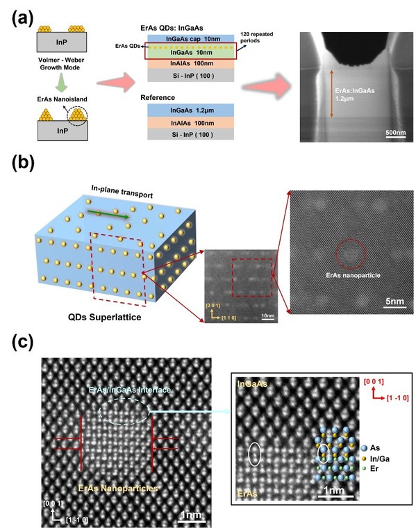
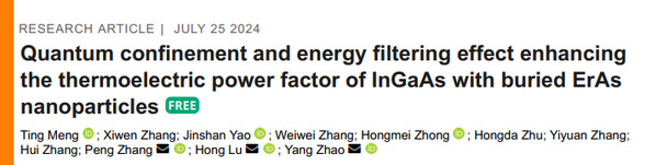
Figure 2. (a) Synthesis of ErAs QDs: In0.53Ga0.47As composite film: Self-assembly growth of nanoisland based on MBE (left), schematic of ErAs QDs: In0.53Ga0.47As composite (middle) and SEM image of the side of the composite film (right). (b) Schematic of the QDs superlattice composite (left): the yellow spheres represent ErAs nanoparticles, and the TEM image of a cross-section of the composite viewed along [1 1 0] (right), showing that the interlayer spacing of each layer of ErAs nanoparticles is approximately 10 nm. (c) HAADF/STEM image of the ErAs QDs: In0.53Ga0.47As viewed along [1 -1 0] (left) and the interface between ErAs and In0.53Ga0.47As (right).
Figure 3. (a) HAADF/STEM images of the ErAs QDs: InGaAs composite with 0.2 (left), 0.5 (middle), and 0.8(right) ML deposition. (b) Carrier concentration and (c) Mobility of the ErAs QDs: In0.53Ga0.47As composite with 0.2, 0.5, and 0.8 ML deposition over the temperature range 250 - 400 K. (d) Schematic (left) and micrograph (right) of the micro lateral in-plane thermoelectric generator device. (e) Schematic of the measurement setup.

Figure 4. (a) Schematic of in-plane carrier transport in the lateral thermoelectric generator device and the TEM image of a cross-section of the composite viewed along [1 1 0]. (b) Seebeck coefficients, (c) Electrical conductivity, and (d) PF of the ErAs QDs: In0.53Ga0.47As composite and reference sample against temperature.

Figure 5. (a) Schematic representation of the density of electron states of the valence band of bulk materials (dashed line) contrasted to low-dimensional materials. (b) Schematic band diagrams before and after accounting for quantum confinement in ErAs QDs assuming the InGaAs barrier.
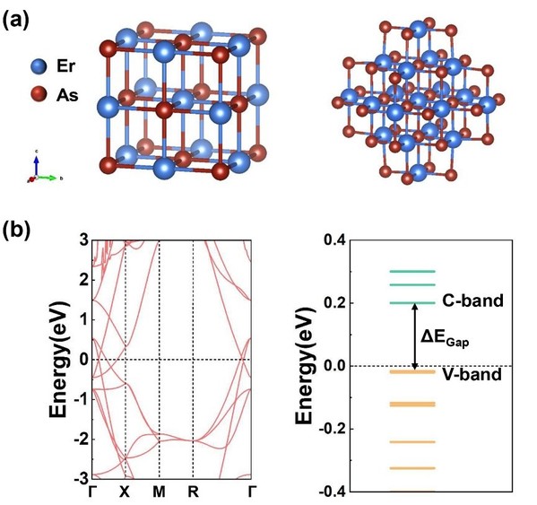
Figure 6. The models (a) and band structures (b) of bulk ErAs (left) and ErAs QD (right), respectively.
中国科学技术大学赵旸教授、张鹏博士后研究员、南京大学芦红教授为论文的共同通讯作者,中国科学技术大学博后孟婷为论文的第一作者。中国科学技术大学张忠教授和汪国睿教授为本工作提供了指导性建议。该研究得到国家重点研发计划、国家自然科学基金、广东省教育厅研究项目和深圳市科技创新委员会项目的支持。
原文链接:
https://doi.org/10.1063/5.0213563